George B. Berry Chair Professor of Engineering
Professor, Mechanical and Aerospace Engineering
Compound Semiconductors
-
X. Song, S. Babcock, C. Paulson, T. Kuech, J. Huang, D. Xu, J. Park, L. Mawst (2008). Nanostructure of GaAs0.88Sb0.10N0.02/InP quantum wells grown by metal-organic chemical vapor deposition on InP, J. Cryst. Growth, 310, 2377-2381.
 |
|---|
 |
The effects of thermal annealing on the emission and microstructural characteristics of GaAs0.88Sb0.10N0.02/InP multiple quantum well (QW) structures were studied by photoluminescence (PL) spectroscopy and transmission electron microscopy (TEM). The results show that the optimum annealing conditions lead to improved PL intensity accompanied by only a small blue shift, contrasting the behavior of GaAsSbN /GaAs multiple QWs, and improved structural uniformity.
-
N. Lazarus, C.D. Meyer, S.S. Bedair, X. Song, L.M. Boteler, I.M. Kierzewski (2013). Thick film oxidation of copper in an electroplated MEMS process, J. Micromech. Microeng. 23, 065017 (9pp).
 |
|---|
Copper forms a porous oxide, allowing the formation of oxide layers up to tens of microns thick to be created at modest processing temperatures. In this work, the controlled oxidation of copper is employed within an all-metal electroplating process to create electrically insulating, structural posts and beams. This capability could eliminate the additional dielectric deposition and patterning steps that are often needed during the construction of sensors, waveguides, and other microfabricated devices. In this paper, copper oxidation rates for thermal and plasma-assisted growth methods are characterized. Time control of the oxide growth enables larger copper structures to remain conductive while smaller copper posts are fully oxidized. The concept is demonstrated using the controlled oxidation of a copper layer between two nickel layers to fabricate nickel inductors having both copper electrical vias and copper oxide support pillars. Nickel was utilized in this demonstration for its resistance against low temperature oxidation and interdiffusion with copper.
-
C.A. Paulson, S. Jha, X. Song, M. Rathi, S.E. Babcock, L. Mawst, T.F. Kuech (2011). The effect of helium ion implantation on the relaxation of strained InGaAs thin films, Thin Solid Films, 520 (6), 2147-2154.
 |
|---|
Previous work on pseudomorphic SiGe on Si has shown that a significant reduction in the threading dislocation density can be achieved through appropriate ion beam processing. Helium ion implantation was used in an analogous study to induce strain relaxation within strained pseudomorphic InGaAs layers on GaAs through the intentional introduction of subsurface damage without the introduction of surface nucleated dislocations and their associated threading segments. Wafers of fully-strained 28 nm thick films of In0.24Ga0.76As were separately implanted with helium doses of 5 × 10¹⁴, 2 × 10¹⁵, and 1 × 1016 cm −2 at 25 keV. These wafers became substrates for additional InGaAs film growth. The final InGaAs films always exhibited lower residual strain as compared to films grown directly on a control substrate of non-implanted GaAs. The broadening of the X-ray peaks indicates an increase in dislocation density within the InGaAs films and the strain relaxation was found to occur with a significant increase in surface roughness. This result stands in contrast to related work on SiGe films on Si where a reduction of the threading dislocation density within a SiGe film was observed. The reaction of the InGaAs/GaAs structure and materials to ion irradiation, with local disturbance to the stoichiometry, could preclude the use of ion beam techniques for realizing a reduction in threading dislocation density during strain relaxation.
-
S. Jha, M. Wiedmann, T Kuan, X. Song, S. Babcock, T. Kuech (2011). Growth behavior and defect reduction in heteroepitaxial InAs and GaSb on GaAs using block copolymer lithography, Journal of Crystal Growth, 315 (1) 91–95.
 |
|---|
Defect reduction in heteroepitaxial growth of GaSb and InAs was achieved using nano-patterned GaAs substrates generated by block copolymer lithography (BCL). The lattice-mismatched growth of both GaSb and InAs on nano-patterned GaAs templates exhibited defect mitigation with few observed threading dislocations, but the growth behavior and surface morphology of the resultant films were very different for the two systems. The strain relaxation process proceeds through the relaxation of the nanoscopic, highly lattice-mismatched islands prior to film coalescence. The growth of GaSb on GaAs templates yielded a smooth, coalesced film whereas large islands were observed for the growth of InAs on such templates. The difference in surface morphology was described in terms of the interaction of adatom surface diffusion and the strain-dependent attachment of these atoms with the growing islands. The morphology can be altered through changes in growth temperature and rate. Nanolithographic patterning can be used as a general technique for integration of lattice-mismatched materials.
-
M. Seehra, V. Singh, X. Song, S. Bali and E. Eyring (2010). Synthesis, structure and magnetic properties of non-crystalline ferrihydrite nanoflakes, Journal of Physics and Chemistry of Solids, 71(9), 1362-1366.
 |
|---|
Synthesis and characterization of the structural and magnetic properties of a 2-line (2L) ferrihydrite (FHYD) sample based on the composition Fe:Al:Cu=100:25:5 are reported. Typical of 2L-FHYDs, this sample also yields the two broad lines in X-ray diffraction and triplet in the 1400–1700 cm −1 range in IR spectroscopy. However, in transmission electron microscopy, nanoflakes of about 5–20 nm size but without any hint of diffraction fringes characteristic of crystalline order were observed. Temperature dependence (2–380 K) of the magnetization M vs. applied field H (up to ±65 kOe) of this non-crystalline ferrihydrite is used to establish a blocking temperature TB ≃20 K, Néel temperature TN ≃365 K and a spin-glass ordering of the surface Fe 3+ spins at TS≃6 K. These magnitudes of TB and TS are considerably smaller than those of a 5 nm undoped 2L crystalline ferrihydrite with TB =70 K and TS =30 K. The fit of the M vs. H data for several T> TB to a modified Langevin function is shown to collapse onto a universal curve yielding a temperature-independent average magnetic moment μP =70(5) μB per nanoflake. Analysis of these parameters obtained from the fits of M vs. H data above TB is used to show that the effective average volume of the nanoflakes is about 1/3 that of spherical 5 nm crystalline 2L-FHYD. It is argued that these lower magnitudes of μP, TB, and TS for the nanoflakes result from their smaller effective volume determined here.
-
J. Kirch, T. Garrod, S. Kim, J. Park, J. Shin, L. Mawst, T. Kuech, X. Song, S. Babcock, I. Vurgaftman, J. Meyer and T. Kuan (2010). InAsyP1−y metamorphic buffer layers on InP substrates for mid-IR diode lasers, Journal of Crystal Growth, 312, 1165-1169.
 |
|---|
The defect-trapping effectiveness of an InAsP metamorphic buffer layer (MBL) design was investigated by studying the light-emission characteristics of InAs quantum wells grown on the MBL, along with structural characterization through SIMS and TEM measurements. Using a fixed recipe for the MBL, several separate confinement heterostructures (SCHs) were studied using 8-band k.p simulations, HRXRD, SEM, optical microscope and variable-temperature photoluminescence. Room temperature PL was observed at wavelengths near 3 μm, although the PL intensity drops significantly for samples with wavelengths longer than 2.85 μm. Laser operation was achieved at 77 K at a wavelength of 2.45 μm and threshold as low as 290 A/cm 2.
-
J. Huang, L. Mawst, T. Kuech, X. Song, S. Babcock, C. Kim, I. Vurgaftman, J. Meyer, A. Holmes (2009). Design and characterization of strained InGaAs/GaAsSb type-II 'W' quantum wells on InP substrates for mid-IR emission, Journal of Physics D-Applied Physics, 42(2) 025108.
 |
|---|
InGaAs/GaAsSb type-II 'W' quantum wells (QWs) grown on InP substrates by metalorganic vapour phase epitaxy were investigated for potential emission wavelengths in the mid-infrared spectral region. Design studies using an 8-band k p Hamiltonian model indicate that emission wavelengths near 3 µm should be achievable without strain relaxation. Improved electron confinement can be achieved by adding higher-energy band gap alloys such as AlAsSb or GaInP around the type-II 'W' active region. Comparisons of the simulations with experiment indicate that photoluminescence (PL) spectra are consistent with a type-II band alignment. 4-period type-II 'W' In0.8Ga0.2As (~4.0 nm)/GaAs0.35Sb0.65 (~1.5 nm) QWs separated by InP (5 nm) or AlAs0.767Sb0.233 (1.5 nm) barrier layers, demonstrate room-temperature PL emission at ~2.1 µm.
-
Rathi, MK; Khandekar, AA; Song, XY; Babcock, SE ; Mawst, LJ; Kuech, TF (2009). High antimony content GaAs(1-z)N(z)-GaAs(1-y)Sb(y) type-II "W" structure for long wavelength emission, J. Appl. Phys. 106, 063713.
 |
|---|
GaAs1−zNz–GaAs1−ySby type-II “W” structures were studied for long wavelength (1300–1600 nm) applications. These structures were grown on a GaAs substrate using metal-organic vapor phase epitaxy. The antimony and nitrogen compositions in the pseudomorphic GaAs1−ySby and GaAs1−zNz were estimated by separately growing GaAs1−ySby–GaAs and GaAs1−zNz–GaAs strained superlattices. X-ray studies indicate that a maximum of y=0.37 antimony can be incorporated in the pseudomorphic GaAs1−ySby film grown using triethyl gallium (TEGa), trimethyl antimony (TMSb) and arsine (AsH3) at the growth temperatures employed. A postgrowth anneal was used to improve the emission intensity but leads to shifts in the emission wavelength. An emission wavelength as long as 1.47 μm was realized using a GaAs1−zNz–GaAs1−ySby–GaAs1−zNz structure
-
J. Huang, D. Xu, X. Song, S. Babcock, T. Kuech, L. Mawst (2008). Growth of strained GaAs1-ySby and GaAs1-y-zSbyNz quantum wells on InP substrates, Journal of Crystal Growth, 310, 2382-2389.
 |
|---|
The metal organic vapor-phase epitaxy (MOVPE) growth conditions and properties of fully strained GaAs1−y−zSbyNz/InP multi-quantum wells (MQWs) are investigated. Higher Sb incorporation within the strained GaAs1−ySby layers was observed when using a higher Sb/(As+Sb) precursor ratio and higher growth temperature. However, lattice-latching effects and the strain values ultimately limit the maximum amount of Sb incorporated. In GaAs1−y−zSbyNz layers, a decrease of AsH3 precursor flux leads to an increase of N and Sb incorporation, whereas an increase of unsymmetrical dimethylhydrazine (U-DMHy) precursor flux leads to an increase of N and a decrease of Sb incorporation. The photoluminescence emission from the GaAs1−y−zSbyNz QW is observed to red-shift with decreasing AsH3 and increasing U-DMHy flux. Sb accumulation at the InP to GaAs1−y−zSbyNz interface is also observed from secondary ion mass spectroscopy analysis, indicating further optimization of switching sequences is required to improve the compositional uniformity of the QW.
-
S. Jha, X. Song, S. Babcock, T. Kuech, D. Wheeler, B. Wu, P. Fay, A. Seabaugh (2008). Growth of InAs on Si substrates at low temperatures using metalorganic vapor phase epitaxy, Journal of Crystal Growth, 310(23) 4772-4775.
 |
|---|
The growth behavior of InAs on Si using metalorganic vapor phase epitaxy (MOVPE) was studied. The large lattice mismatch of InAs to Si, ∼12%, results in island formation under typical MOVPE growth conditions, which prevents the development of the thin coherent films of InAs needed for high-speed device applications. The growth of InAs at low temperature is expected to lead to rapid nucleation and low surface mobility, resulting in the formation of a coherent film at low thicknesses. This study explored the growth behavior of InAs on Si at low temperatures, i.e. <350 °C and varying V/III ratio. InAs films were grown on {1 0 0}-, {1 1 1}- and {2 1 1}-oriented Si substrates using trimethyl indium, tertiary butyl arsine and AsH3. Small islands ranging from 15 to 30 nm form on the samples at growth temperatures <325 °C. Subsequent annealing of this thin layer at 600 °C for 5 min leads to island coarsening. High-resolution X-ray diffraction, atomic force microscopy and scanning electron microscopy were used to characterize InAs layer grown on Si.
-
T. Kuech, A. Khandekar, M. Rathi, L. Mawst, J. Huang, X. Song, S.E. Babcock, J.R. Meyer and I. Vurgaftman (2008). MOVPE growth of antimonidecontaining alloy materials for long wavelength applications, Journal of Crystal Growth, 310, 4826-4830.
 |
|---|
GaAs-based heterostructures comprised of GaAs1−xNx–GaAs1−ySby ( x<0.03, y<0.35) multiple quantum wells (MQW) that utilize ‘W’-shaped type-II transitions have potential for realizing high-performance monolithic VCSELs and edge-emitting lasers with low temperature sensitivity in the 1.55 μm wavelength region. Metal-organic vapor-phase epitaxy (MOVPE) growth of GaAsSb is complicated by both thermodynamically driven phase separation and kinetic effects that arise from incomplete thermal decomposition of methyl- and hydride precursors at typical growth temperatures. The impact of growth chemistry on the formation of strained and pseudomorphic films was studied through the growth of relaxed GaAsSb films and multi-period pseudomorphic GaAsSb/GaAs superlattices. Trimethyl- and triethyl-gallium and trimethyl- and triethyl-antimony were used in a variety of combinations. The observed variations of the Sb incorporation efficiency for relaxed and strained films with growth conditions are not predicted by the existing thermodynamic models of the growth, indicating a coupling of the surface growth chemistry and the strain-induced changes in the surface stoichiometry. Through modification of the growth chemistry and process conditions, an extended range of Sb incorporation was realized as well as enhanced control over the alloy composition in strained layers. These achievements lead directly to an extended wavelength range in type-II MQW structures.
-
D. Xu, J. Huang, J. Park, L. Mawst, T. Kuech, X. Song, S. Babcock (2007). Annealing of dilute-nitride GaAsSbN/InP strained multiple quantum wells, Applied Physics Letters, 91, 191909.
 |
|---|
The thermal annealing of GaAsSbN/InP strained multiple quantum wells (MQWs) grown by metal organic chemical vapor deposition was investigated. Photoluminescence peak intensity and linewidth changes indicate a significant improvement in optical quality of the GaAsSbN/InP MQWs upon annealing. We find no significant annealing-induced blueshift of the optical transitions, which confirms the theoretical expectation that a change in the nearest-neighbor configuration nitrogen atoms has negligible effect on the band gap of GaAsSbN. The evolution of (400) x-ray diffraction rocking curves with thermal treatment of the samples was consistent with the constituent redistribution in the GaAsSbN QW.
-
J. Huang, D. Xu, J. Park, L. Mawst, T. Kuech, X. Song, S. E. Babcock, I Vurgaftman, and J. R. Meyer (2007). Characteristics of strained GaAs1-ySby (0.16 ≤ y ≤ 0.69) quantum wells on InP substrates. Journal of Physics D: Applied Physics, 40 7656-7661.
 |
|---|
Pseudomorphic GaAs1−ySby quantum wells with 0.16 ≤ y ≤ 0.69 on (0 0 1) InP substrates have been grown using metal–organic chemical vapour deposition. High resolution x-ray diffraction and transmission electron microscopy analysis are used to quantify the layer thicknesses and compositions. Studies of the optical properties suggest that a transition from type-I to type-II band alignment occurs at an antimony concentration of approximately y = 0.30. The interband optical transition energies simulated using a ten-band k p Hamiltonian are compared with the experimental values deduced from photoluminescence spectroscopy. The valence band offset bowing parameter is evaluated in the context of the experimental transition energies. For low Sb-contents, reasonable agreement (<7% deviation) is achieved between theory and experiment for the primary optical transitions. However, at higher Sb-content, there is significant deviation between the measured transition energies and the k p based theory, possibly a result of a non-ideal interface and/or heterogeneous ternary well.
-
A. Khandekar, J. Y. Yeh, L.J. Mawst, X. Song, S. E. Babcock and T. F. Kuech (2007). Effects of Ga- and Sb-precursor chemistry on the alloy composition in pseudomorphically strained GaAs1−ySby films grown via metalorganic vapor phase Epitaxy, Journal of Crystal Growth, 303, 456-465.
 |
|---|
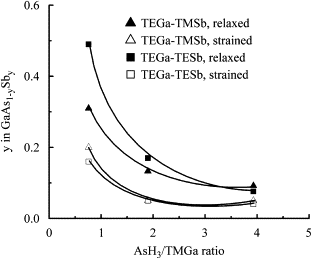
GaAs-based multiple quantum well (MQW) heterostructures comprised of metastable alloys such as GaAs1−ySby-GaAs1−zNz have potential for realizing high-performance and low temperature-sensitivity lasers in the 1.55 μm wavelength region. However, strain-induced ‘lattice-latching’ and Sb-surface segregation effects limit the Sb-mole fractions in the pseudomorphically strained GaAs1−ySby layers to y⩽0.2. The effect of Ga- and Sb-precursor chemistry and the growth temperature on the Sb-incorporation efficiency in strain-relaxed and strained, pseudomorphic GaAs1−ySby films was studied using metalorganic vapor phase epitaxy. Both trimethyl- and triethyl-gallium (TMGa and TEGa) and trimethyl- and triethyl-antimony (TMSb and TESb) were used as Ga- and Sb-precursors, in four different source combinations, with arsine. The Sb-mole fraction in the strained GaAs1−ySby films was found to be lower than that in the relaxed films for all of the precursor chemistries. The highest Sb-incorporation rates were found with the TEGa-based growth with strained-layer compositions up to y∼0.48 being obtained for the growth conditions employed. The results were discussed in terms of the strain-related thermodynamic effects and the chemical kinetics of precursor surface decomposition for the different precursor chemistries.
-
A. Khandekar, J. Y. Yeh, L. J. Mawst, X. Song, S. E. Babcock, T. F. Kuech (2007). Growth of strained GaAs1-ySby layers using metalorganic vapor phase Epitaxy, Journal of Crystal Growth, 298, 154-158.
 |
|---|
The growth of pseudomorphically strained GaAs1−ySby layers with high Sb-mole fractions of y⩾0.35 are desired on GaAs substrates for making lasers and detectors in the mid-infrared range. The effect of gas-phase precursor chemistry on the strained-layer Sb-incorporation efficiency in metalorganic vapor phase epitaxy (MOVPE) was determined using four combinations of ethyl- and methyl-Ga and Sb precursors. The Sb-mole fractions in the strained GaAs1−ySby layers were found to be lower than those in relaxed films due to the strain-induced ‘lattice-latching’ effects. The Sb-mole fraction in the strained GaAs1−ySby layers decreased with the increasing AsH3/Ga ratio for all the precursor chemistries. Higher Sb-incorporation efficiencies were observed for the ethyl-Ga chemistries. The experimental results were discussed in terms of lattice-latching effects, Sb-segregation phenomena and different decomposition kinetics for various precursor chemistries.